I had an idea after watching both BenEater’s and 3Blue1Brown’s videos on hamming codes: what if they were baked into the instruction set of a CPU? This would mean that each instruction in a program could be checked and corrected against single bit errors natively, and provide more reliable operation.
Something like a spacecraft or rover, which are subjected to significant amount of radiation (and thus also bit flips) could benefit from this. With hamming codes built into the instruction set, one of the bits in any instruction can be flipped, and the CPU will still understand the instruction and execute it. For 16 bit instructions, this isn’t practical as the hamming codes take up 5 bits. For 64 bits or 128 bits though, this is a lot more feasible, requiring only 7 and 8 bits for hamming codes, respectively.
While I have made an assembler before, this is basically the first CPU I’ve ever designed and built from scratch, and it was a lot of fun.
ISA
To keep things simple, I wanted to design an instruction set architecture (ISA) with the minimum capability to calculate the Fibonacci sequence to 233, which is the maximum value that can fit within 8-bits. Going off of my knowledge about some of the basic instructions required for an ISA, this is the instruction set I came up with. Due to the limit of 11-bits per isntruction, and not wanting instructions that take up multiple addresses, I had to limit it to 4 8-bit registers with 16 8-bit slots of RAM. I also had to limit it to 256 instructions total due to the program counter (pc) also only being 8-bits.
| instr. | operation | mach. code | flag |
|---|---|---|---|
NOP |
No operation | 000_XXXX_XXXX |
|
AND RR SS |
And S and R, store in R | 001_0000_RRSS |
x |
OR RR SS |
Or S and R, store in R | 001_0001_RRSS |
x |
ADD RR SS |
Add R to S, store in R | 001_0010_RRSS |
x |
SUB RR SS |
Sub S from R, store in R | 001_0011_RRSS |
x |
INC RR |
Increment R | 001_0100_RR00 |
x |
DEC RR |
Decrement R | 001_0101_RR00 |
x |
CMP RR SS |
Compare R with S | 001_1000_RRSS |
x |
LDD RR DD |
Load from data D into R | 010_DDDD_00RR |
|
LDR RR SS |
Load from D based on S into R | 010_00SS_01RR |
|
STD RR DD |
Store R in data D | 010_DDDD_10RR |
|
STR RR SS |
Store R in addr by 4 bits of S | 010_00SS_11RR |
|
JMP RR |
Jump to address in R | 011_0000_00RR |
|
JMP RR CC |
Jump to address in R if C | 011_CCCC_00RR |
|
LDI RR VV |
Load immediate V into R | 1RR_VVVV_VVVV |
These are the comparison values given to JMP for a conditional jump.
| CMP | CC | CMP | CC |
|---|---|---|---|
| any | 0 | <= (unsigned) | 7 |
| zero | 1 | = | 8 |
| negative | 2 | > (signed) | 12 |
| carry | 3 | < (signed) | 13 |
| > (unsigned) | 4 | >= (signed) | 14 |
| < (unsigned) | 5 | <= (signed) | 15 |
| >= (unsigned) | 6 |
Here is the basic code for calculating the Fibonacci sequence, commented with what each instruction does.
main:
    ; Load register 0 with the value 1
    LDI 0 1
    ; Load register 1 with the value 1
    LDI 1 1
    ; Load register 2 with the address of fib
    LDI 2 fib
    ; Load register 3 with the value 0
    LDI 3 0
    ; Store the value in register 0 at the RAM address
    ; pointed to by the value in register 3
    STR 0 3
    ; Increment the value in register 3
    INC 3
    ; Store the value in register 1 at the RAM address
    ; pointed to by the value in register 3
    STR 1 3
    ; Decrement the value in register 3
    DEC 3
fib:
    ; Load into register 0 the value in the RAM address
    ; pointed to by the value in register 3
    LDR 0 3
    ; Increment the value in register 3
    INC 3
    ; Load into register 1 the value in the RAM address
    ; pointed to by the value in register 3
    LDR 1 3
    ; Add the values of registers 0 and 1 and store them in register 1
    ADD 1 0
    ; Load register 2 with the address of end
    LDI 2 end
    ; Jump to the address stored in register 2
    ; if the carry flag is set from the addition
    JMP 2 3
    ; Increment the value in register 3
    INC 3
    ; Store the value in register 1 at the RAM address
    ; pointed to by the value in register 3
    STR 1 3
    ; Decrement the value in register 3
    DEC 3
    ; Load register 2 with the address of fib
    LDI 2 fib
    ; Unconditionally jump to the address in register 2
    JMP 2
end:
    ; Unconditionally jump to the address in register 2
    JMP 2
Simulator
I wrote a simulator to make sure my ISA was good enough before moving on to implementing it in an assembler or hardware, where changes would take longer to implement. It works by reading all the lines of the input file and parsing them as text to instructions, without encoding or decoding them in hamming 16/11. To make this easier to work with than the last assembler I wrote, I implemented this as a Python class with a command-line wrapper, instead of just as a Python script. This also made the code cleaner and easier to understand.
Here is it in action:
Using this I was able to weed out the parts of my ISA that were problematic and truly nail down what I was looking for. I also used this to debug my Fibonacci assembly program by adding the ability to step through each line, viewing the values of the pc, flags, registers, and RAM. I also added the ability to break only at certain points in the code by adding a ;break comment at a specific line.
I added an interactive mode where instructions can be passed in one at a time, but this wasn’t as useful as I thought it would be (as JMP wouldn’t have anywhere to go).
I had to add a limit to the number of instructions to prevent infinite loops if the end of the file is never reached. This is easy to change though (just change the instr_limit variable of the simulator class).
If there are no breakpoints and --step is not passed, it will run until the end and print the values, then exit.
When I was happy with this, I decided to move on to the assembler.
Assembler
The assembler shares a similar architecture to that of the simulator, where the assembly file is read and split by line, then each individual line is parsed as an instruction. It is also implemented as a Python class with a command-line wrapper (and I’m considering going back and redoing my Intel 4004 assembler in this fashion because it’s so much better).
The main issues I ran into were getting the hamming codes to come out correctly, and I tried reimplementing it several times but I couldn’t get it to work. I resorted to the amazing hamming-codec Python library written by Daniel Antrim, which worked perfectly.
I had it output as a file of ASCII hex representing the machine code as that’s the best format for working with VHDL. I also had it pad 0000’s to fill out the space for the 256 instructions. It can also output the resulting hex representation for each instruction both before and after hamming encoding.
$ ./ecccpu_asm.py -i ../asm/fib.asm -o ../hdl/rom.bin --verbose

           main:
401  8118    LDI 0 1
501  a00a    LDI 1 1
60a  c0a6    LDI 2 fib
700  e111    LDI 3 0
23c  47d1    STR 0 3
2e8  5c90    STD 0 14
14c  28d7    INC 3
23d  47de    STR 1 3
2e9  5c9f    STD 1 14
15c  2bd4    DEC 3
           fib:
234  4747    LDR 0 3
14c  28d7    INC 3
235  4748    LDR 1 3
124  2442    ADD 1 0
616  c366    LDI 2 end
332  6633    JMP 2 3
14c  28d7    INC 3
23d  47de    STR 1 3
2e9  5c9f    STD 1 14
15c  2bd4    DEC 3
60a  c0a6    LDI 2 fib
302  6035    JMP 2
           end:
302  6035    JMP 2
HDL
I decided to use VHDL as that’s what I am most comfortable with right now. I utilized the open source fpga toolchain (GHDL, Yosys, Nextpnr, Icestorm) for simulation and synthesis.
rom
The first thing written was the rom, which was generated by reading in values from the hex file generated by the assembler. This was verified with a testbench to observe the correct values were in the rom. I did run into an annoying bug that took a bit to figure out though, in that if there wasn’t an empty line at the end of the hex file, the rom would fail to read the last line. This was fixed by changing the assembler to add one.
hamming decoder
Funnily enough, I had already written VHDL entities for encoding/decoding/fixing hamming codes last summer after watching BenEater’s videos on the topic, following his designs for how they worked. For this project, I simply pulled that code and dropped it in.
alu
The alu operates on all instructions beginning with 001. It takes in an operation and two arguments, and returns the result. It also handles setting the flags.
cpu
The CPU works in a two stage process. The first stage takes the decoded instruction from the rom and executes different things based on it, with a bunch of if and case statements for different parts of the instruction. The second stage fetches a new instruction from the rom, decodes it, and also transfers any data from the ALU to the specified register if there was an instruction in stage 1 that required the ALU. I originally had the data transfer from the ALU to whatever register on the falling edge of the same clock, but this didn’t work as Yosys doesn’t supprt multi-clock flip flops (yet).
I decided to have the flags not clear until another instruction was executed that set the flags, for simplicity sake.
For fun, I also decided to have ram address 14 be an output and ram address 13 be an input. For the Fibonacci program, I had it write the Fibonacci numbers to this output as it went along, so that I could see them when I tested it on real hardware.
Results
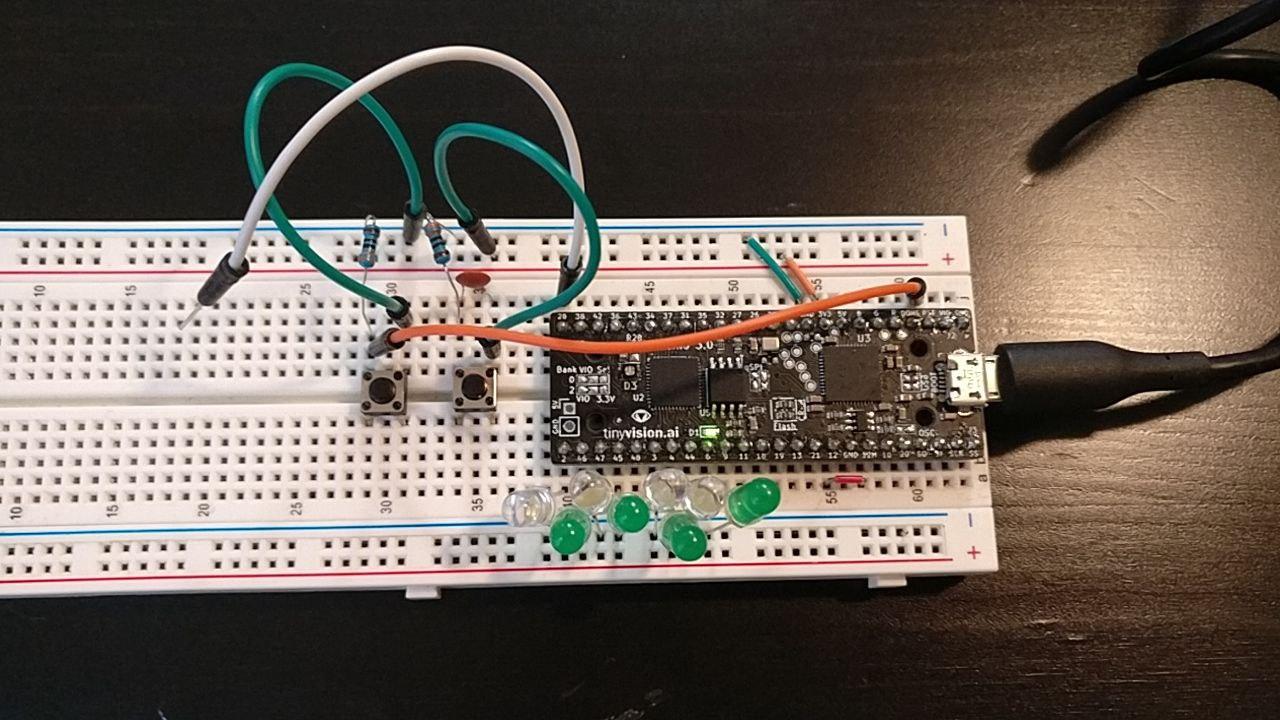
After finishing testing the HDL code, I was able to successfully run it on the Upduino v3.0. I connected 8 LEDs to the values of RAM address 14, and connected a pushbutton to the clock. While the pushbutton didn’t exactly work, often giving garbage results (for some unknown reason), holding the wire or connecting it directly to the 12 MHz clock on board worked really well. I also connected another button to the reset pin of the Upduino to quickly reset the CPU.
Overall I am pretty happy with the results, and definitely have learned a lot more about how CPUs work, and am excited for whatever projects I decide to work on next.
Some possible improvements that could be made in the future include:
- Switching to 32-bit or 64-bit instruction sizes, which would allow for this to be more of a general purpose ISA
- Look into if it’s possible to co-op another ISA (like RISC-V) into a hamming code ISA, to allow for more general purpose programs to be compiled for it
- Add instructions to this ISA for multiple ROMs, IO registers, etc.
The source code is available here and is licensed under the MIT License.
Sources
- How to initialize RAM in VHDL from a file
- dcode was really helpful in debugging my hamming code implementation
- 3Blue1Brown’s video on hamming codes
- BenEater’s video on hamming codes in hardware, from which I borrowed the schematic for how to encode / decode hamming codes in hardware