Overview
The goal for this project was to develop a GPU-like core in VHDL for the Upduino v2 and v3. This would include a 60Hz 320x200 or 640x480 resolution output with read/write frame and color buffers, using PWM to increase the color depth. The color buffer would use color cells similar to those of the Commodore 64. Here is a block diagram showing how it would operate:

- HSOSC generates the specific pixel clock signal
- VGA generates the specific timings to output to the display
- BUTLER takes the pixel position information and generates the correct color/frame addresses
- COLOR/FRAME_BUFFER simply holds the information needing to be displayed
- INFUZER takes the color and frame data and gives the specific PWM RGB data for that pixel
However, due to limitations inherent in the Upduino, the full design was not realized. A simpler design with a text buffer was built instead. Here is a block diagram showing how it operates:

- HSOSC generates the specific pixel clock signal
- VGA generates the specific timings to output to the display
- BUTLER takes the pixel position information and generates the correct text addresses
- TEXT_BUFFER holds the ASCII value for the letter at that position
- FONT holds the specific sprite data for that letter
Design
VGA
A VGA monitor displays an image by stepping through each pixel of the display one by one and lighting up that pixel whatever color it needs to be. VGA has 5 active signals: HSYNC, VSYNC, RED, GREEN, and BLUE.
RED, GREEN, and BLUE are analog signals from 0.0v to 0.7v that hold the brightness of each color.
HSYNC and VSYNC are digital signals that tell the monitor when to move to the next line (HSYNC) and to the top of the screen (VSYNC). Whenever it is time for a new line, the specified signal is activated - this is the sync part of a VGA timing. Because VGA was originally designed when CRTs were the monitor of choice, it had to work around its limitations. Due to this, there are buffers around the sync pulse that give the CRT monitor time to move to the next line. These are the front porch and back porch part of a VGA timing. Here is a diagram showing how these timings are used, to scale for a 640x480 display.

Here is a block diagram of the designed VGA core. It operates by having two counters - one for the horizontal position (col) and another for the vertical position (row) - and setting HSYNC and VSYNC to on when either is in the sync position. RED, GREEN, and BLUE are simply passed through and not included here for clarity.

Frame/Color Buffer
A frame/color buffer is a section of memory that holds the color for every pixel on the display, and can be changed without needing to rewrite everything.
I had intended to use color cells very similar to the ones used on the Commodore 64, and for an explanation on how these would have worked, please see this excellent video by the 8-Bit Guy.
It is very important to take into account how much color you want or need within a project, and how much space you need to hold that color. For this, I made this chart showcasing the different ways of storing color information. It is a balance between color depth and wasted space.
| Color Depth | Bit Setup | Total Space | Wasted Space | # Colors | # Pins |
|---|---|---|---|---|---|
| 3-bit | RGBX |
4 bits | 1 bits | 8 | 3 |
| 4-bit | RGGB or RGBI |
4 bits | 0 bits | 16 | 4 |
| 6-bit | RRGG BBXX |
1 bytes | 2 bits | 64 | 6 |
| 8-bit | RRRG GGBB |
1 bytes | 0 bits | 256 | 8 |
| 9-bit | RRRG GGBB BXXX XXXX |
2 bytes | 7 bits | 512 | 9 |
| 12-bit | RRRR GGGG BBBB XXXX |
2 bytes | 4 bits | 4096 | 12 |
| 15-bit | RRRR RGGG GGBB BBBX |
2 bytes | 1 bits | 32,768 | 15 |
Another way to do color is by having a color palette, where your color buffer could simply point to a specific color in a buffer instead of having to store the color information itself. By doing this, one could reduce the size of the color buffer while also having access to different colors, both at the cost of not having all the colors of the palettes bit-depth available at once and using more output pins.
Text Buffer
This buffer operates differently from the frame/color buffers; one buffer holds a value pointing to the specific character to use for that position (such as an ASCII value), and another holds the information for what that character looks like (such as a font). This way, it is possible to point to a specific predetermined character or sprite, instead of having to code it manually every time.
Pulse-Width Modulation (PWM)
Because the color lines are analog and the FPGA only operates on digital (without resorting to using either more pins or an DAC), there needs to be some way to convert the color information in the color buffer into an analog signal. One method of achieving this would be turning a signal on and off rapidly with specific on/off times, then use a low-pass filter to smooth everything out. Then, by altering the amount of time the signal is on vs off, a varying analog signal can be generated.
The PWM signal would be created by generating a clock speed that’s N/2 times bigger than the pixel clock for a PWM level of 1/N, and using logical functions to combine these depending on the level required. For a PWM with increments of 1/8, you’ll need to generate a clock speed that’s 4 times higher than your pixel clock.
Here are the different clocks and the logic expressions that generate each PWM level from said clocks.

Low Pass Filter
Given all that information, here is the low pass filter I designed in LTSpice. R4 is the internal resistance of the monitor. There would be one of these circuits per color channel.

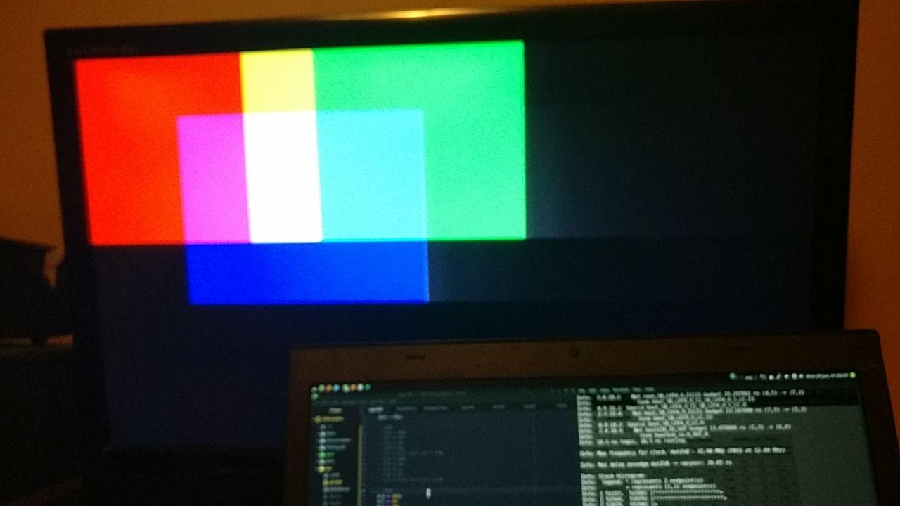
Here is how the simulation circuit performed in PWM levels, left to right in 1/8 increments starting with 1/8. I could not find any information about the known slew rate of the Upduino, nor did I have the proper equipment to determine it experimentally, so this is using an ideal slew rate of 0. It is evaluating a 40 MHz signal.

Limitations
There are some limitations of the Upduino that I had to consider after designing the processes above. Unfortunately, to accommodate these limitations, the scope of the project had to be changed.
Memory
For instance, a 320x200 resolution display has 64,000 pixels, and assuming a black and white screen (no color palette), this would take up 64,000 bits or 8 kbytes. The Upduino has 125 kbytes of SPRAM (Single-Port RAM) and 15 kbytes of DPRAM (Dual-Port / EBR RAM), and for this frame buffer DPRAM is preferable.
This isn’t too bad, but given most modern monitors don’t support this resolution anymore, and some color would be nice, I also did calculations for other resolutions and color options.
| Horizontal Res. | Vertical Res. | Pixels | Color Method | Total Bytes |
|---|---|---|---|---|
| 320 | 200 | 64,000 | Greyscale | 8 KB |
| 320 | 200 | 64,000 | 8x8 Color Cells, 1,000 3-bit depth | 8.5 KB |
| 640 | 480 | 307,200 | Greyscale | 38.4 KB |
| 640 | 480 | 307,200 | 8x8 Color Cells, 4,800 3-bit depth | 40.8 KB |
| 1024 | 768 | 786,432 | Greyscale | 98.3 KB |
| 1024 | 768 | 786,432 | 8x8 Color Cells, 12,288 3-bit depth | 835.3 KB |
Very quickly we run out of space, and due to wanting to use DPRAM where possible, this only leaves 320x200 as a viable resolution if we want to use frame and color buffers. For this reason, I had to drop using frame/color buffers in favor of manual control and text buffers. Manual control would mean that whatever program is using the VGA core would have to set the color of each pixel every frame, instead of writing to a frame buffer and only changing it when necessary. While it is worse for more complex projects, it works really well for simple designs, especially when memory-limited.
Clocks
I had to determine whether the Upduino could handle the clock speeds necessary to drive the VGA display. During tests I performed on prototypes talked about later on, the Upduino could only output 4:3 resolutions with a max pixel clock of 60-70 MHz.
| Horizontal Res. | Vertical Res. | Refresh Rate | Pixel Clock |
|---|---|---|---|
| 160 | 100 | 60 Hz | 1 MHz |
| 320 | 200 | 60 Hz | 5 MHz |
| 640 | 480 | 60 Hz | 23.75 MHz |
| 800 | 600 | 60 Hz | 38.25 MHz |
| 800 | 600 | 75 Hz | 47.12 MHz |
| 1024 | 768 | 60 Hz | 63.5 MHz |
| 1920 | 1080 | 30 Hz | 79.75 MHz |
| 1920 | 1080 | 60 Hz | 173 MHz |
The PWM has to happen at very high speeds as well. For instance, a 640x480 display requires a pixel clock of ~24 MHz, meaning each pixel’s color is only being determined within a ~42 ns duration, and 1/8 PWM will require a clock speed of 96 MHz.
Even more of an extreme example is 1920x1080, which requires a pixel clock of 173 MHz, meaning a pixel time of ~5.8 ns, and 1/8 requiring a clock speed of 690 MHz. This is simply not possible on the Upduino. For this reason I chose to stick to 3-bit color depth, for 8 colors total.
Pins
While it is also possible to provide color using multiple pins per channel and a voltage divider, I decided to go against this due to the limited number of pins available on the Upduino; I wanted to make sure it would use as little pins as possible to make it easier to integrate with other projects. With 9-bit color, for instance, the Upduino could output 512 different colors to the display, but it would also take up ~1/3 of all the pins available.
It is possible other FPGAs may be able to overcome these limitations and fully realize the original design; however, I had to adjust the design to fit the intended hardware.
Prototyping
VGA Adapter
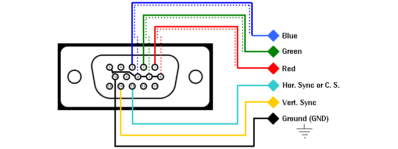
The VGA adapter was fairly simple to build. I bought a VGA connector and soldered the correct wires following this pinout.
PLL and VGA timings
The PLL is a special block inside the UP5K that allows you to generate any clock speed between 16 MHz and 275 MHz from any clock speed between 10 MHz and 133 MHz. This is especially useful for the VGA entity where the pixel clocks required don’t line up nicely with the 48 MHz internal clock. There are two tools I used to generate the timings required for the VGA and PLL, being cvt, provided by xrandr, and icepll, provided by the Icestorm Project. When using the PLL, I would highly recommend using an external clock (such as the 12MHz one on the v3 or a seperate clock altogether) as it can be unstable, especially on the Upduino v2[1].
Testing
Using icepll and cvt, I was able to test various resolutions on the Upduino v2 and v3 on two different monitors (an Envision L24H898 and an Acer H213H). When the resolution didn’t work, thee display would either be completely black or would complain about it being an unsupported format. Here are the different resolutions that worked:
| Resolution | Pixel Clk | v2 | v3 |
|---|---|---|---|
| 640x480 | 25.125 MHz | ✓ | ✓ |
| 800x600 | 49.5 MHz | ✓ | ✓ |
| 1024x768 | 65 MHz | ✓ | |
| 1280x720 | 74.25 MHz | ||
| 1366x768 | 86 MHz | ||
| 1280x1024 | 109 MHz | ||
| 1920x1080 | 148.5 MHz |
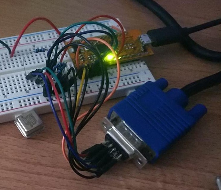
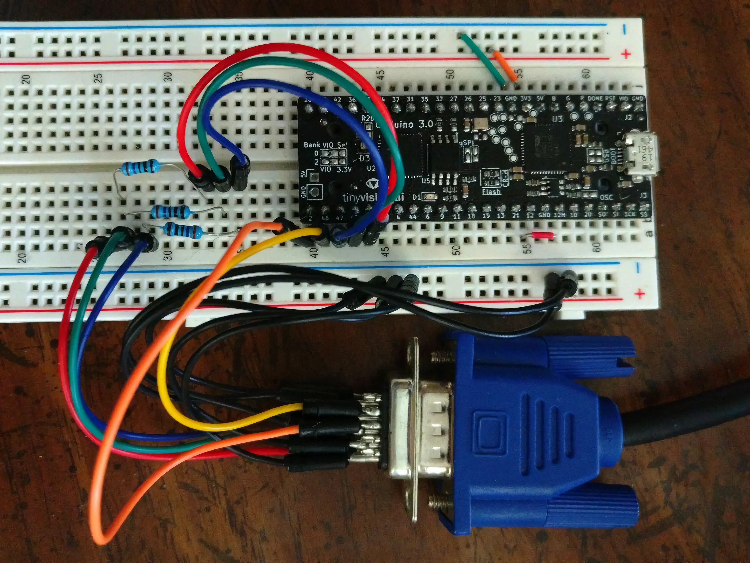
Initial assembly
This is what it looked like when completed and wired to the Upduino. Note that I added 270 ohm resistors in series with each color line bring the 3.3v of the Upduino down to the max voltage of the color line at 0.7v. This helped in reducing the noise on the display. Unfortunately, due to using the internal clock and the grounding issues with the v2 itself, the display would cut out every minute or so, and there was significant noise on the display. On top of this, if there were too many changes in the color (such as too many letters), the signal quality would get progressively worse until no signal would be present at all.
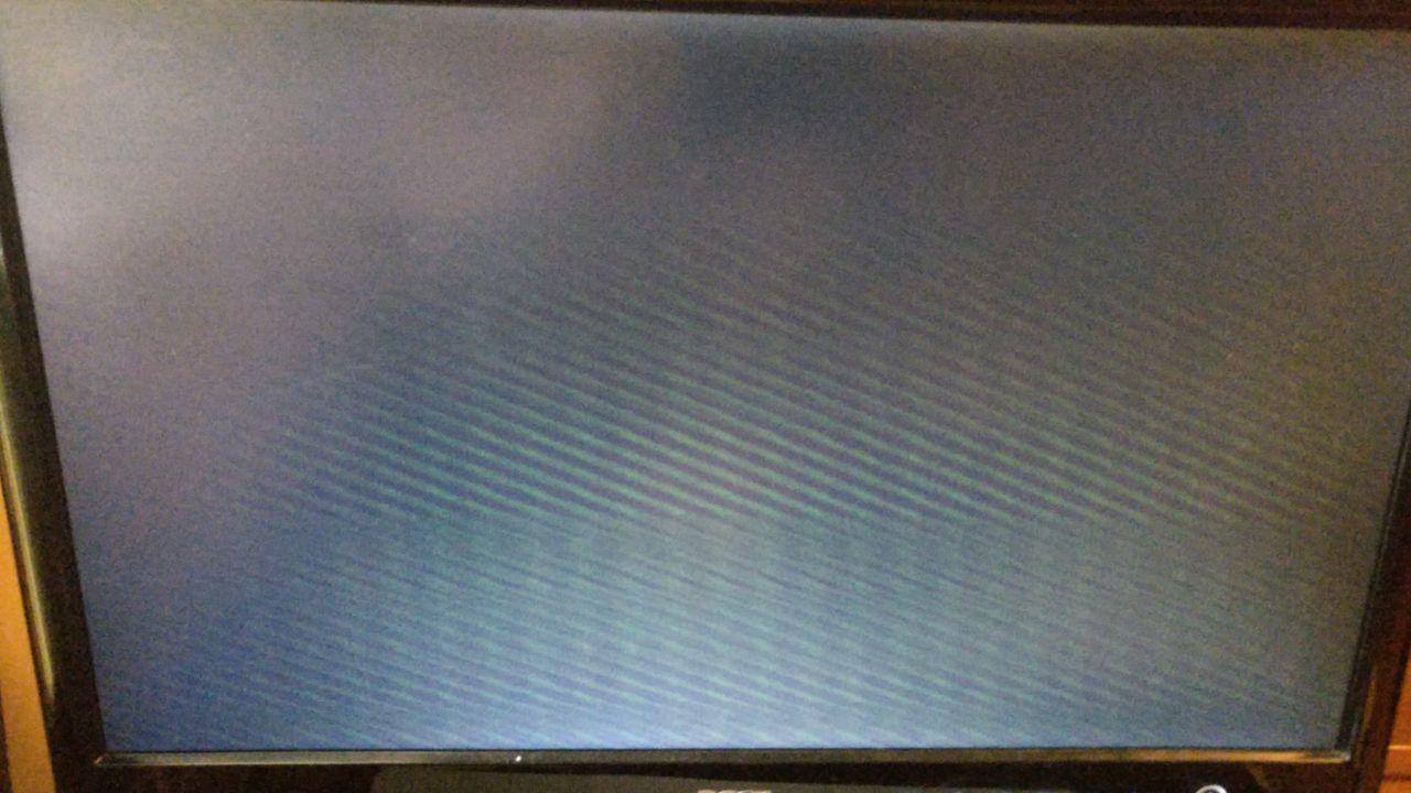
One thing to note is that the color lines need to be pulled to 0v when not on the display, otherwise the image on the screen becomes extremely distorted and unintelligible. This problem stumped me for a week or so until I figured it out.
Be careful what else is attached to the circuit aswell, as it can sometimes cause severe ghosting. This was caused when I used my oscilloscope and had the probe on one of HSYNC or VSYNC.
When testing the text buffer, I had to increase the size of the letters due to the amount of left/right static in the image.
Final Assembly
The final assembly looks exactly the same as the initial assembly, except I used the Upduino v3 instead of the v2. This is also using the external 12MHz clock on the Upduino v3 instead of the internal clock. The benefit to this is that the signal no longer drops out every minute, and there is a significant reduction in noise. Unfortunately, there is still a little bit of left/right static present on the right side of the screen, even if greatly reduced, and depending on what is being displayed, it will be distorted with vertical and/or horizontal lines. It is possible that this is due to being attached to a breadboard and that the jumper wires aren’t shielded to protect from interference, and also because the buffer may be being synthesized into logic instead of the on-board RAM.
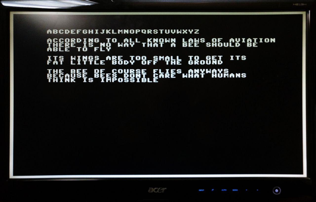
Here is an example of what the final text buffer design is capable of. The letters are written in ASCII into a buffer ahead of time, and when the row/col are over that letter, it send that letter to the font which displays the correct pixel on the screen.
Recap
If I were to continue this project, I would have continued to work on solving the noise/line bugs I experienced with using the text buffer through interfacing with the RAM manually instead of leaving it to Yosys. I would have also worked on adding write capability to the text buffer.
Even though I did not succeed in my original idea, I would still consider this project a success. I had a lot of fun working on this project, and I definitely learned a lot; there is much more that goes into showing an image on a screen than what it seems like on the surface. I hope this served to help you learn more as well.
Source code
Here is the complete source code for this project. It is licensed under GPLv3. I used the open source toolchain for this project (Icestorm + Yosys + NextPNR + GHDL).
Helpful Resources
- Ground trampolines and Phase Locked Loops by Venkat Rangan
- VGA driver for Altera UP1 board by Rob Chapman